Researchers have created an innovative transparent layer that sits between two insulating materials. This material allows electrons to move in a two-dimensional plane at room temperature, with their spins (an inherent property of electrons called intrinsic angular momentum) all pointing in the same direction. This breakthrough could significantly speed up data transfer between different parts of electronic devices and increase the amount of data that can be stored in quantum devices.
The need for attaining new functionalities in modern electronic devices has led to the manipulation of property of an electron called spin degree of freedom along with its charge. This has given rise to an altogether new field of spin-electronics or ‘spintronics’.
For decades, spintronics held theoretical promise, but its exotic behaviours seemed like science fiction. Concepts like spin currents and manipulation remained elusive. However, with the development of advanced materials and fabrication techniques, particularly at the nanoscale, scientists are now creating condensed matter systems that exhibit these very properties. This opens doors to a new era of spintronic devices with functionalities beyond traditional electronics.
Scientists at Institute of Nano Science and Technology (INST) an autonomous research institution of Department of Science and Technology (DST) situated at Mohali India, have produced for the first time a transparent conducting interface between two insulating materials with room temperature spin polarized electron gas which allows for see-through devices with efficient spin currents.
Prof. Suvankar Chakraverty and his group at INST have produced a 2D Electron Gas (2DEG) with room temperature spin polarization at the interface composed of chemicals LaFeO3 and SrTiO3. They grew super lattices and hetero structures of oxide materials to realize new and exotic two-dimensional electron gas at the interface of two insulating oxides that could be useful for next generation quantum devices.
The research supported by a grant from the DST-Nanomission and Board of Research in Nuclear Sciences (BRNS) in the form of a sophisticated, custom-made instrument called a combinatorial pulsed laser deposition setup, was published in the journal ‘Physical Review B’ in the Letters section.
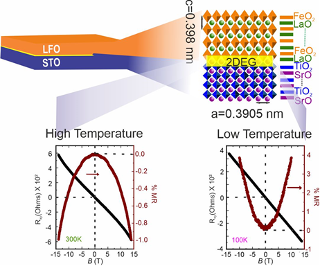
The interface of the two insulating materials LaFeO3-SrTiO3 that could host two-dimensional electron gas is very different from the previously reported interfaces with SrTiO3. It for the first time exhibited unusual phenomena of room temperature. Due to the spin polarization the electrons, which are aligned in a particular direction (in a magnetic field) experienced less resistance (negative magnetoresistance) and deflected the current sideways (anomalous Hall effect). This was due to structural transition of SrTiO3 at interface with temperature. Such features have great significant in spintronics quantum-device applications.
Spin carries additional information compared to just charge. By manipulating spin in transparent materials, Chakraverty and his group unlock new possibilities for light-controlled spintronics – functionalities impossible with traditional charge-based devices. Transparency allows for integration of spintronic devices within existing displays or solar cells.
A transparent phone screen that processes information with spin currents, or a solar cell that generates electricity and manipulates spin for advanced functionalities opens a door to entirely new device architectures.
Realization of conducting transparent oxide interface with spin polarization at high temperature, may open up a new field of quantum-device physics especially in the field of transparent spin-electronics quantum-devices, dissipation less electronics and quantum devices applicable for next generation data storage media and quantum computers.
Publication details: https://doi.org/10.1103/PhysRevB.109.L201114
For more details Prof. Suvankar Chakraverty (suvankar[dot]chakraverty[at]gmail[dot]com) can be contacted.

Figure showing the interface with lattice parameters, the lower panel of the figure is showing the magnetoresistance and Hall resistance at low (100K) and high temperature (300 K).


