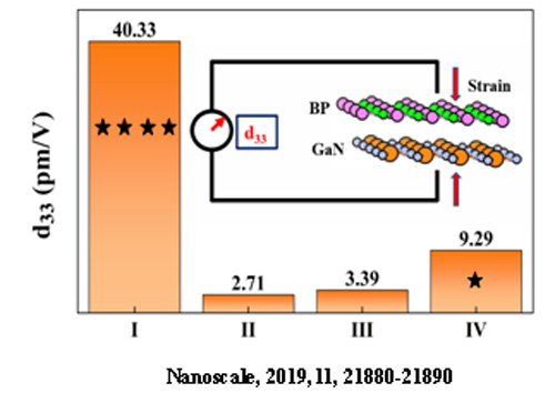
 Researchers from Institute of Nano Science and Technology (INST), Mohali an autonomous institute under the Department of Science & Technology, have made computer based designs of nano-materials with superhigh piezoelectricity which can be the building blocks of futuristic nano-electronics for applications like ultrathin, next-generation nano-transistors.
Piezoelectricity is the generation of electricity in certain materials upon application of pressure. Its applications have eased our daily lives through the use of lighters, pressure gauge, sensors and so on.
Piezoelectricity in 2D materials was first predicted theoretically in 2012 and later observed and confirmed experimentally in monolayer in 2014. Since then, there has been a surge in research interests in piezoelectricity in graphene-like two-dimensional (2D) materials, thereby leading to the exploration of piezoelectricity in 2D materials or avenues to induce or enhance piezoelectricity in 2D materials. However, most of the 2D materials reported till date mainly show in-plane piezoelectricity; however, for device-based applications, out-of-plane piezoelectricity is very much desired and sought after.
Prof. Abir De Sarkar & his Ph.D. student, Manish Kumar Mohanta in their recent publications in Nanoscale and American Chemical Society have demonstrated induction of superhigh out-of-plane piezoelectricity via stacking one monolayer over the other in the 2D nanostructure.
The induction of this phenomenon is based on two-dimensional van der Waals heterostructure (vdWH) comprising of 2D monolayers, The vdWH is a new approach in materials design where different monolayers having complimentary properties are combined together to surmount their intrinsic limitations.When two monolayers are stacked over one another to constitute a vdWH, various factors affect the electronic properties. The dipoles arising at the interface due to the large charge density difference between the two constituent monolayers extend out into the interlayer region, which result in such an ultrahigh value in out-of-plane piezoelectricity.
In their work funded by the Department of Science and Technology under Nanomission and Council of Scientific and Industrial Research (CSIR), India the researchers have predicted that predicted that the the out-of-plane piezoelectric coefficient of the materials designed by them will reach as high as 40.33 pm/V, which is very high as compared to the bulk materials, such as wurziteAlN (5.1 pm/V), GaN (3.1 pm/V), commonly used in industry.
With the continued trend in the miniaturization of electronic devices, there is a growing demand for superfast ultrathin nanodevices and nanotransistors. The nanostructures could be an essential ingredient or building block in constructing these kinds of nanodevices. The superfast nanoelectronics can be realized from the ultrahigh charge carrier mobility in ultrathin nanostructures. The carrier mobility of the designed nano-materials have been found to exceed that for silicon and therefore, the ultrathin nanostructures thereby providing an insight into the building blocks in futuristic nano-electronics.
The computational materials can motivate experimentalists to fabricate nano devices with the desired functionality. Transistors used in the mother board of Computers and Laptops are getting tinier and thinner with the passage of time. So, piezoelectric nanomaterials may be utilized in these ultrathin, next-generation nano-transistors through a synergistic coupling between piezoelectricity and electronics.
They have published these two papers in leading International Journals, Nanoscale (I.F. 6.97) and ACS Applied Materials and Interfaces (I.F. 8.456).
Details:
(1) Mohanta, M. K.; Rawat, A.; Dimple; Jena, N.; Ahammed, R.; De Sarkar, A. Superhigh Out-of-Plane Piezoelectricity, Low Thermal Conductivity and Photocatalytic Abilities in Ultrathin 2D van Der Waals Heterostructures of Boron Monophosphide and Gallium Nitride. Nanoscale2019, 11 (45), 21880–21890. https://doi.org/10.1039/C9NR07586K.
(2) Mohanta, M. K.; Rawat, A.; Jena, N.; Dimple; Ahammed, R.; De Sarkar, A. Interfacing Boron Monophosphide with Molybdenum Disulfide for an Ultrahigh Performance in Thermoelectrics, Two-Dimensional Excitonic Solar Cells, and Nanopiezotronics. ACS Appl. Mater. Interfaces2020, 12 (2), 3114–3126. https://doi.org/10.1021/acsami.9b16866
References:
- Duerloo, K.-A. N.; Ong, M. T.; Reed, E. J. Intrinsic Piezoelectricity in Two-Dimensional Materials. J. Phys. Chem. Lett.2012, 3 (19), 2871–2876. https://doi.org/10.1021/jz3012436.
- Wu, W.; Wang, L.; Li, Y.; Zhang, F.; Lin, L.; Niu, S.; Chenet, D.; Zhang, X.; Hao, Y.; Heinz, T. F.; Hone, J.; Wang, Z. L. Piezoelectricity of Single-Atomic-Layer MoS2 for Energy Conversion and Piezotronics. Nature2014, 514 (7523), 470–474. https://doi.org/10.1038/nature13792.
- Zhu, H.; Wang, Y.; Xiao, J.; Liu, M.; Xiong, S.; Wong, Z. J.; Ye, Z.; Ye, Y.; Yin, X.; Zhang, X. Observation of Piezoelectricity in Free-Standing Monolayer MoS2. Nat. Nanotechnol.2014, 10, 151.
- Hong, X.; Kim, J.; Shi, S.-F.; Zhang, Y.; Jin, C.; Sun, Y.; Tongay, S.; Wu, J.; Zhang, Y.; Wang, F. Ultrafast Charge Transfer in Atomically Thin MoS2/WS2 Heterostructures. Nat. Nanotechnol.2014, 9, 682.
- Mohanta, M. K.; Rawat, A.; Dimple; Jena, N.; Ahammed, R.; De Sarkar, A. Superhigh Out-of-Plane Piezoelectricity, Low Thermal Conductivity and Photocatalytic Abilities in Ultrathin 2D van Der Waals Heterostructures of Boron Monophosphide and Gallium Nitride. Nanoscale2019, 11 (45), 21880–21890. https://doi.org/10.1039/C9NR07586K.
- Mohanta, M. K.; Rawat, A.; Jena, N.; Dimple; Ahammed, R.; De Sarkar, A. Interfacing Boron Monophosphide with Molybdenum Disulfide for an Ultrahigh Performance in Thermoelectrics, Two-Dimensional Excitonic Solar Cells, and Nanopiezotronics. ACS Appl. Mater. Interfaces2020, 12 (2), 3114–3126. https://doi.org/10.1021/acsami.9b16866.
- Jena, N.; Dimple; Behere, S. D.; De Sarkar, A. Strain-Induced Optimization of Nanoelectromechanical Energy Harvesting and Nanopiezotronic Response in a MoS2 Monolayer Nanosheet. J. Phys. Chem. C2017, 121 (17), 9181–9190. https://doi.org/10.1021/acs.jpcc.7b01970.


