


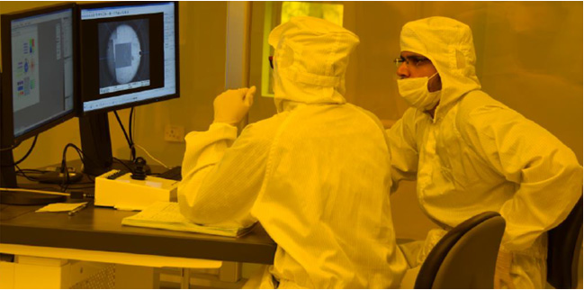
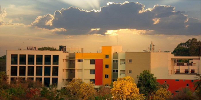
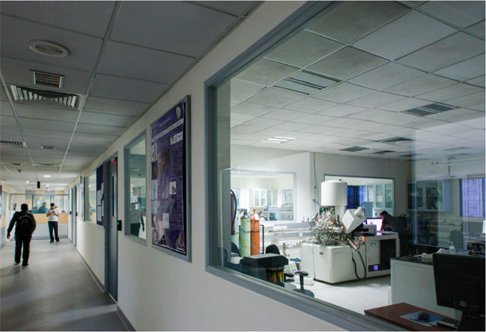
 The Centre for Nano Science and Engineering (CeNSE) lab at IISc, Bengaluru, is a buzz with activity. The dynamic interdisciplinary team at the state-of-the-art nanofabrication facilities (Fabs) brought together by the efforts of the Principal Scientific Advisor (PSA) to the Govt. of India, Ministry of Electronics and Information Technology (MeitY), and the Department of Science and Technology (DST), is passionately working ontechnologies such as in sensing, IoT, microfluidics, photonics, and nanomaterials for solutions in agriculture, healthcare, safe drinking water, and energy harvesting.
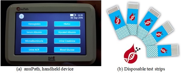
The interdisciplinary team that set up the research facilities in a span of seven years has already brought out several technologies and products. The research on electrochemical biosensors has led to “lab-on-palm” or multi-analyte handheld diagnostic device, “anuPath”. This is the only product in the world capable of performing 5 blood tests and 3 urine tests.The research on MEMS has yielded inexpensive pressure sensors for aerospace applications such as helicopters and light combat aircraft.
Besides these, the enthusiastic team at CeNSE has several technologies like the Envirobat, airSense, Gallium Nitride-based power electronics, nanomotors, the “Ocean” reactor for the CVD of graphene, etc., under its belt. Armed with these, the team has already ensured that India does not miss the nano-technology bus like it did in case of the micro-electronics bus.
Point-of-care Diagnostics: Electrochemical biosensors, ‘lab-on-palm’
CeNSE has developed electrochemical biosensors for early diagnosis and management of multiple chronic diseases including Diabetes, Anemia and Malnutrition, Liver and Kidney diseases. In particular, the group has developed novel receptors to sense multiple biomarkers including Hemoglobin, HbA1c, Serum Albumin, Glycated Albumin, Glucose, Microalbuminuria, Urine creatinine, and the Albumin-to-Creatinine Ratio.
In Diabetes management, the group has been able to develop, for the first time, a novel paradigm for time-differential glycemic indexing through the simultaneous measurement of Glucose (instant blood sugar), Glycated Albumin (2 weeks average blood sugar) and HbA1c (3 months average blood sugar). Serum Albumin sensing is enabled by exploiting the copper-binding property of albumin. This is the first demonstration of albumin measurement from whole blood, without the need for separating serum from whole blood. Glycated albumin sensing is performed using the boronic affinity principle in conjunction with copper chemistry. Hemoglobin sensing is done using aza-heterocyclic receptors to ensure highly accurate sensing over the entire physiological range. HbA1c is measured with the boronic affinity principle in conjunction with an aza-heterocyclic receptor. The Creatinine-iron binding property is used to develop an accurate urine creatinine sensor.
The technology has been translated into a commercial product, through a start-up. Prof. Bhat and his student, Dr Vinay Kumar, cofounded PathShodh Healthcare Pvt Ltd, in the year 2015, to translate this research into a useful product for societal impact. By December 2016, the product was fully developed and qualified through extensive clinical validation, and a manufacturing facility was set-up for scale-up and field deployment. The technology is protected by 1 issued US patent and 3 pending US patents, 3 pending European patents, 3 pending Japanese patents, 1 pending Chinese patent, and 7 pending Indian patents.
The features of this “lab-on-palm” device include novel non-enzymatic (and hence robust) disposable test strips, minimally invasive finger-prick testing, extremely low sample volume (micro-litre), user-friendly touch-sensitive GUI customizable to any language, Bluetooth connectivity to android phones and the cloud, capability to map all the test results of individuals with the Aadhar card number, thereby enabling a revolutionary health repository for data mining and data analytics.
Pressure Sensors for aviation
Developing low-cost pressure sensors to detect minute pressure differences for aviation is an achievement that the CeNSE team is proud of. CeNSE has developed a complete suite of MEMS pressure sensors for reading the absolute pressure, gauge pressure, and differential pressure in the range of tens of millibars to 600 bars. These sensors use a thin silicon diaphragmas a mechanical structure that deforms under applied pressure. The deformation is measured by a set of silicon piezoresistors used in a Wheatstone bridge configuration that converts the deformation into voltage readout. The sensitivity and the range of sensing depend on the design and successful realization of the diaphragm and the peizoresistors. In addition, the sensing element requires MEMS packaging with interface electronics and application-specific casing and port design; the sensors have been tested extensively for aerospace applications.The comprehensive effort on pressure sensors – from design to fabrication, packaging, and testing – was led by two senior faculty members of CeNSE, K.N. Bhat and M.M. Nayak.
The pressure sensors are inexpensive, simple to fabricate, compact, lightweight, highly sensitive and accurate, while consuming little power. They also offer excellent repeatability and the ability to build redundancy in same size, as they lend themselves to mass production.
The product has been successfully launched commercially. This is the first commercial MEMS product from India. Right now, the users are strategic sector players in aerospace whose requirements are in hundreds per year.
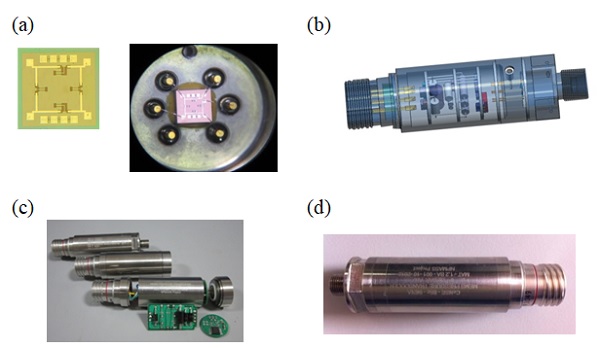
Pressure sensors developed at CeNSE (a) Bare sensor die, sensor die on a header (b) Internal view of full assembly (c) Fully packaged 1.2 bar pressure transducer (d) A fully packaged gauge pressure transducer
Thriving research programs in various domains of nano-science and technology
CeNSE has thriving research programs in various domains of nanoscience and technology, aided by the wherewithal to make significant contributions to these domains and to the wider society. An important initiative has been to engage with the country’s strategic sector, resulting in close collaboration with DRDO, DAE, and ISRO, with numerous projects in CeNSE funded by these agencies of the Govt. Given the capabilities installed, CeNSE has naturally engaged with industry, with a pioneering Industry Affiliate Program that counts major Indian and multinationals as actively engaged members.
A Business Incubator in Nanotechnology is being established with support from the Govt. of Karnataka, which will soon host start-ups. Some of them are expected to build on R&D conducted in CeNSE, where the emphasis has not only been on high-quality academic research and publications, but also on technology development, witness the considerable portfolio of patent filings. A CeNSE course on Entrepreneurship attracts students from all over campus.
The journey so far
 It was the early 2000’s and the country had famously missed the “microelectronics bus”. At the Indian Institute of Science, IISc, a premier institution in the vaunted “silicon valley” of India, there was no laboratory for fabricating silicon devices, even those with 100-micron features. It was then that a small, interdisciplinary band of young faculty members – alarmed but motivated – led by Rudra Pratap (Mechanical Engineering) and Navakanta Bhat (Electronics Engineering), initiated a discussion among a few colleagues about establishing a modern “Fab” for the development and study of micro and nano devices, lest India miss the nanotechnology bus, too. Along with two senior colleagues, S Mohan (Instrumentation) and S AShivashankar (Materials Science), they evolved a proposal to set up a Centre of Excellence in Nanoelectronics.
It was at this time that Dr. Chidambaram, the Principal Scientific Advisor (PSA) to the Govt. of India, understood that it was incumbent on the Govt. urgently to support the setting up of state-of-the-art nanofabrication facilities (Fabs) at academic centres in the country. Through discussions, he judged that it would be best to establish two of them simultaneously, at IISc and IIT-Bombay, with adequate funding from the Dept. of Electronics and Information Technology, DeitY. Encouraged by the PSA and led by Dr. Phadke, Group Coordinator, R&D in Electronics Group and Dr Uttam , Head, Nanotechnology Division", in 2005, DeitY approved ₹ 50 Cr in funding each for setting up Centres for Excellence in Nanoelectronics (CEN) at IISc and IITB as a 5-year project.
 At IISc, the “Fab team” presented an ambitious vision to the Institute administration, of creating best-in-class “cleanroom” laboratories and anchoring them in a new department. Prof. P Balaram, Director, and Prof. N Balakrishnan, Associate Director, offered their unstinted support for establishing a new academic department in 2010, which was named “Centre for Nano Science and Engineering” (CeNSE) to reflect the interdisciplinary nature of its genesis and future. The team expanded by recruiting two more key members: P S Anil Kumar (Physics) and Srinivasan Raghavan (Materials Science). Work increased and so did the commitment, the output, and the achievements.
The team at CeNSE, IISc, is driven by its commitment to excellence in the field of science, to contribute to society and to make the country proud of its nano-science and technology. A proud passenger of the world’s nanotech bus now, they dream of the day when they will be directing its route.
")


")


