


A new material that possesses high transparency in the visible and NIR (near infra-red) range and is also highly conducting could have promising applications as transparent electrodes (TEs) in the optoelectronic devices.
Transparent electrodes (TEs) are one of the critical components of the optoelectronic devices and are based on materials which can be tuned to being simultaneously optically transparent and electrically conductive. These fundamentally contrasting attributes of this component make it applicable in areas extending from energy generation and emission devices to gas sensors, low-emissivity windows, thermoelectric generators, and flat panel displays.
The most widely used TEs are based on metal oxide thin films, like, Sn (tin) doped indium oxide (ITO), F (fluorine) doped tin oxide (FTO), and Al (aluminium) doped zinc oxide (AZO), with ITO being one of the extensively used TE in the optoelectronic industry because of its high optical transparency in the visible range and low electrical resistivity.
Note here that visible photons constitute only a small fraction of the solar spectrum, and operation of an optoelectronic device in this region could consequently limit its performance.
The development of infrared (IR) transparent electrodes (specifically in the near-infrared range) is crucial for improving the efficiency of certain optoelectronic devices and opening up applications in other emerging areas, like IR photodetectors, IR switching devices, sensors, and modulators for telecommunication. Along with the relatively low NIR transparency of these three metal-oxide TE, scarcity, high cost and cytotoxicity of In, toxicity of F, and poor chemical stability of ZnO necessitate the development of new high-NIR transmittance TE along with high visible transparency.
In a breakthrough study, researchers at Indian Institute of Technology Gandhinagar (IITGN) have developed a material that possesses high transparency in the visible and NIR range and is also highly conducting, which has promising applications as TE in the optoelectronic devices. Moreover, its abundance (hence cost-effectiveness), non-cytotoxicity, chemical inertness, and high NIR transparency, along with highly-visible transmittance, could make it a promising alternative over the conventionally used TEs.
Microscopic images, the layer thicknesses, and uniformity of these films were crucial during the fabrication as well as optimization process. For these tests, the scientists used the Analytical Scanning Electron Microscope (JEOL make) procured through the Fund for Improvement of S&T Infrastructure in Universities and Higher Educational Institutions (FIST) programme of the Department of Science and Technology (DST). A patent has already been filed on this work.
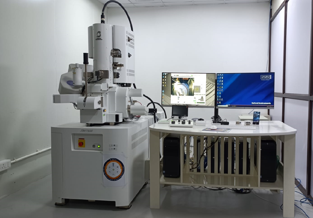
Fig. 1 Analytical SEM setup at IIT Gandhinagar
In this study, Group-V doped TiO2 thin films were synthesized. A film thickness of around 80 nm shows an electrical resistivity and optical transmittance in the visible range that is comparable with the commercially available transparent electrodes of ITO, AZO, and FTO. Additionally, this film shows very good transmittance in the NIR range, with an average transmittance of 88%, which is far superior to the currently available metal oxide electrodes by around 33%. Moreover, use of this electrode could maximize the transmittance of visible and NIR range photons to the optoelectronic devices, thus enhancing the device performance as well as enabling new applications.
Ref: Emila Panda, Shivam Shukla, Transparent electrode and a process for its preparation, Date of filing: 16/09/2022, Patent application no: 202221053057.
")


")


