


An Indian scientist has indigenously developed a low-cost semiconductor manufacturing process and used it to design integrated circuits (ICs) that can handle voltages up to 20 V. These developed high voltage devices along with the processes were integrated into the CMOS (Complementary Metal Oxide Semiconductor) process flow of Semi-Conductor Laboratory (SCL), Mohali in a cost-effective manner.
Electronics in satellites need different supply voltages, need power management ICs (PMICs), and battery management ICs. The PMICs need a CMOS technology that can offer a wide range of voltages with high performance. However, the Semiconductor Lab’s 180nm CMOS technology, which is planned to be used for fabricating the clock drivers and PMICs for future satellites, only supports voltages up to 3.3V.
To solve this problem, Dr. Nihar Ranjan Mohapatra, Professor at the Indian Institute of Technology Gandhinagar, along with his team at Nanoelectronics Devices and Circuits Lab (nano- DC Lab) of IIT Gandhinagar, has augmented the available CMOS technology (at SCL) with the capability to manufacture semiconductor devices capable of handling voltages up to 20 V which are crucial for the PMICs. This work was done with support from the Advanced Manufacturing Technologies Program of the Department of Science & Technology, Government of India. He has also filed a national patent for the same.
The technology, which is in the 4th stage of the Technology Readiness Level, could be used to design clock drivers, high voltage switches, power management ICs (PMICs), and battery management ICs. The testing of the developed devices has been carried out at IIT Gandhinagar and Semiconductor Laboratory, Mohali and Space Application Centre, Ahmedabad.
Once qualified, this technology will be an asset for space and defense applications. According to ‘India Power Management IC Market Forecast and Opportunities 2020’, the power management IC (PMIC) market in India is expected to witness double-digit growth at a CAGR over 10% during 2015-2020. Besides the traditional industry segments like consumer electronics and mobile devices, the demand for PMICs is also expected to grow within other application sectors like IT and office automation, networking, and telecom equipment.
However, because of the absence of an indigenous manufacturer and indigenous technology, the industry is entirely dependent on the imports from other countries. Many a times, the strategic sectors like space and defense have to wait for a long time to get access to a state-of-the-art CMOS-DMOS technology (used for PMICs) from outside foundry. The indigenous development of the CMOS-DMOS technology and the availability of low-cost semiconductor processes in India will open up more design activities and encourage technical start-ups in PMICs.
Patent details: A SOURCE SIDE UNDERLAP LATERAL DMOS TRANSISTOR AND METHOD OF FABRICATING THEREOF, Indian Patent, Application No. 201921014956, 2019.
Publication details:
- Kumari Neeraj Kaushal and Nihar R. Mohapatra, “A zero-cost technique to improve ON-state performance and reliability of power LDMOS transistors”, IEEE Journal of Electron Devices Society (IEEE JEDS), Vol. 9, pp. 334-341, 2021.
- Shubham Patil, Kumari Neeraj Kaushal, Mandar Bhoir and Nihar R. Mohapatra, “Physics-Based Parameter Extraction Methodology for Channel Doping Gradient (CDG) LDMOS Transistors Based on HiSIM-HV2 Model”, IEEE Electron Device Technology and Manufacturing (EDTM) Conference, Chengdu, China, March 9-12, 2021.
For more details, contact Dr. Nihar Ranjan Mohapatra, Professor, Indian Institute of Technology Gandhinagar (96386 54805, nihar[at]iitgn[dot]ac[dot]in).
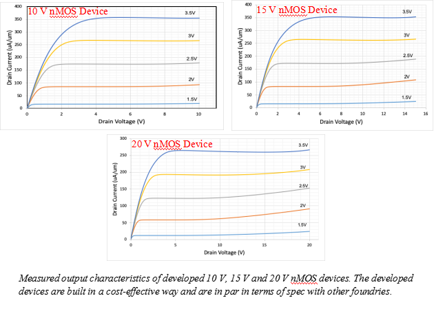
Measured output characteristics of developed 10 V, 15 V and 20 V nMOS devices. The developed devices are built in a cost-effective way and are in par in terms of spec with other foundries.
")


")


