


Scientists have developed a synthetic material design that can control the temperature at which a material can overcome electronic ‘traffic jams’ an transition from an electrical insulator to a con-ductor, setting the ground for an electronic switch that is more efficient than a transistor.
Generally, most commonly encountered materials are either electrical conductors (such as copper or aluminium) or electrical insulators (such as plastic and paper). Correlated electron materials are such a class of materials which undergo an electronic transition from an insulator to a metal. However, these transitions work as a function of temperature making them less useful in devices such as an electronic switch that usually operate at a constant temperature (usually room temperature). Further, these transitions occur at a temperature that might not be relevant for room temperature operation.
Scientists at IISc, in collaboration with scientists from Japan, Denmark and the United States have proposed a synthetic material design that enables them to control the temperature at which the transition occurs. The teams of scientists, including Prof. Naga Phani and his colleagues at the solid state and structural chemistry unit, at IISc Bangalore, proposed and demonstrated a three-layer structure that comprises of an ‘active’ channel layer that undergoes the metal to insulator transition, a charge reservoir layer that can ‘drip’ electrons into the active layer and control the temperature at which the transition occurs, a charge-regulating spacer layer between the active layer and the reservoir layer which regulates the flow (or ‘drip’) of electrons from the reservoir layer to the active
layer.
Preparing nanometer-thick atomically smooth layers of these materials is critical for the success of this work. Such thin layers are prepared by a technique called pulsed laser deposition which allows atomic layer control on the preparation of these layers – in effect this is similar to spray-painting with atoms. The researchers used an atomic force microscope (AFM), funded by the DST-FIST program, for qualifying the quality of their layers. The authors performed extensive AFM studies to arrive at the right conditions (such as temperature, pressure, growth rate) for developing this synthetic stack of materials.
For this research published in the journal Nature Communications, the scientists used an oxide of the element of Vanadium (VO2) to show that greater than a billion-trillion electrons per a cubic centimeter of VO2 (>1021 electrons/cm3) can be ‘dripped’ into the VO2 layer. Usually, the addition of as many electrons to any material is achieved by a process called ‘doping’ where an ‘impurity’ (called a dopant) is added to a high purity material. However, such a process also alters the regular periodic arrangement of atoms in a high purity crystal and affects its utility. The novel synthetic materials layer that the researchers proposed in this work eliminates the necessity to add an ‘impurity’ to modify the materials’ properties. Further, the authors developed an easy to synthesize and replicate amorphous-layer design for the reservoir and the spacer layers.
This work enables the study and control of properties of these exotic materials that can be both insulators and conductors. Further this work shows that electronic ‘traffic-jams’ that lead to insulating behavior in these materials are quite stubborn and challenge our understanding of correlated electron materials. Scientists are looking forward to extending this research to study and develop other exotic materials such as superconductors. They are also interested in exploring the possibility of developing new devices that harness ‘phase’ transitions in these synthetic structures. The purely electronic control of phase transitions proposed by researchers in this work can also enable the study of quantum critical points and phase transitions at interfaces with possible applications in classical and quantum computing.
Publications: https://www.nature.com/articles/s41467-023-41816-3
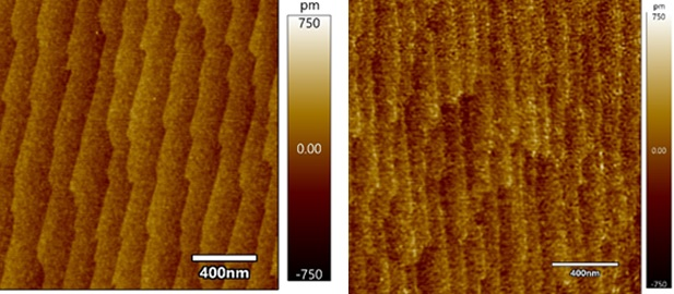
Figure 1: Steps of atomic planes imaged using an atomic force microscope (Cypher-ES) funded by DST-FIST.
")


")


