Scientists have found a new way to increase the efficiency of nitride semiconductors used in thermoelectricity, plasmonics, and artificial synaptic devices.
A fundamental challenge of certain type of nitride semiconductors such as p-type scandium nitride (ScN) in realizing high-efficiency electronic device applications is their low hole mobility or the ability of a hole to travel across it in the presence of an applied electric field. ScN is an emerging III-nitride semiconductor with recent significant interests for its high thermoelectric power factor, metal/semiconductor superlattice development, infrared polaritonic nature, optoelectronic artificial synaptic device, and metal-semiconductor junction diode called Schottky diode junction for thermionic applications. Although ScN has the potential for applications in various fields, the low hole mobility is a significant impediment in realizing its device performance.
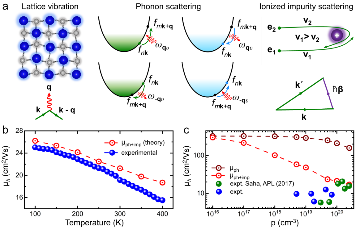
Researchers in Bengaluru’s Jawaharlal Nehru Centre for Advance Scientific Research (JNCASR), an autonomous institute of the Department of Science and Technology, have designed a strategy to improve the hole mobility in semiconducting p-type scandium nitride (ScN). Sourav Rudra and co-worker Dheemahi Rao in JNCASR along with Prof. Samuel Poncé from Université catholique de Louvain, Belgium, investigated for the first time the origin of low hole mobility in ScN and suggested a novel pathway to enhance it. They demonstrated the strain-induced enhancement of hole mobility in p-type ScN using a major formalism to determine transport properties of metal and semiconductors called state-of-the-art Boltzmann transport equation (BTE) calculations. Under this strain engineering method, the split-off hole band with lower effective mass goes above the heavy hole band of higher effective mass. As a result, biaxially tensile strained ScN has lower valence band effective mass for the topmost valence band which will increase the carrier mobility in the hole transport process.
“Our work marks significant progress in not only identifying the causes for low hole mobility in nitride semiconductors, but we also propose and experimentally verify a practical method to increase the hole mobility with strain engineering. This work will significantly advance our quest to develop high-efficiency devices with semiconducting ScN and nitride heterostructures in general. Several device technologies such as plasmonics, thermoelectrics / thermionic energy conversion, and brain-inspired computing will benefit from this work,” said Prof. Bivas Saha, Associate Professor at the Jawaharlal Nehru Centre for Advanced Scientific Research.
The work published in Nano Letters, an ACS publication can further motivate experimental research to achieve high-performance electronic devices in the future. ScN has recently shown great potential for thermoelectricity, plasmonics, artificial synaptic devices, and Schottky barrier diode applications. Hole doping and enhancement of hole mobility in ScN are important for ScN’s potential implementation in almost all types of devices to make them more efficient.
Publication : https://doi.org/10.1021/acs.nanolett.3c02350

Figure 1: Major types of scattering effects that govern the low hole mobility in p-type ScN. The temperature-dependent mobility, calculated from the ab initio Boltzmann transport formalism matches well with the experimental result at 1020 cm-3 carrier concentration.


