Electrical noise, considered a nuisance, becomes bearers of information if decoded carefully. Scientists have fabricated an experimental field effect transistor ( transistor that uses an electric field to control the flow of current in a semiconductor) that can measure its own defects by extracting information from fluctuations in electrical resistance in a graphene sheet. This can help in designing low-noise electronic transistors.

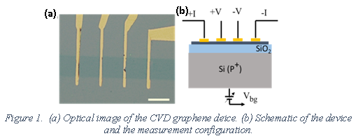
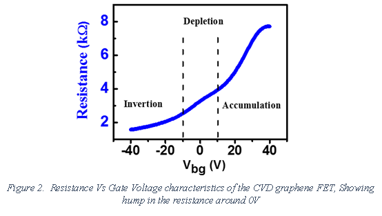
Flicker noise occurring due to the scattering of electrons from any mobile defects is an important factor that influences the sensitivity of field effect transistors (FET) and affects their performance. Ph.D. scholars at the Condensed Matter and Materials Physics Department of S.N. Bose National Centre for Basic Sciences used these fluctuations to detect the role of remote defects in the experimental device they fabricated. The device consists of a large area of graphene grown by a technique called Chemical Vapor Deposition (CVD) placed on a lightly doped Silicon (Si)/silicon-di-oxide (SiO2) substrate. In contrast to earlier studies where a heavily doped substrate was used, the team from SNBNCBS, an autonomous institute of the Department of Science and Technology (DST), used a lightly doped silicon substrate. The substrate and the graphene layer acted like a parallel plate capacitor, and by application of a positive gate voltage (used to control the current of a transistor) on the substrate, charges can be accumulated on the graphene sheet.

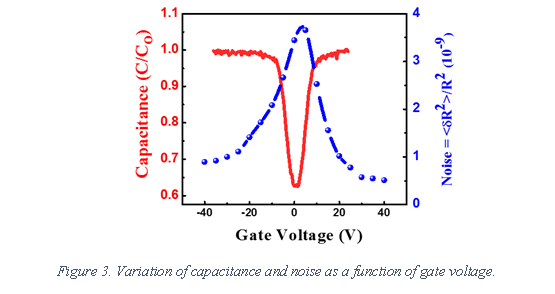
While in previous studies, it was observed that only interfacial defects (within 1-2 nm from graphene) generate electrical noise in field effect devices, in this study, researchers showed that mobile defects close to the depletion region can generate huge noise, which can degrade the performance of the device. They used this noise as the source of information for detecting defects, paving the way for designing low-noise electronic transistors for controling the flow of current in a semiconductor. This study can be useful in integrating graphene with existing silicon technology in the industry, where typically moderately doped substrates are used. The study brings to light that substrates have a huge role to play in the operation of large-area graphene FETs, for which the operating region should be specified for getting the best results. It may lead to integration of graphene transistors with silicon.

Publication link: https://doi.org/10.1021/acsami.2c14499


